- 您现在的位置:买卖IC网 > Sheet目录489 > NTHD2102PT1G (ON Semiconductor)MOSFET PWR P-CH DUAL 8V CHIPFET
�� �
�
�NTHD2102P�
�Power� MOSFET�
�?8.0� V,� ?4.6� A� Dual� P?Channel� ChipFET� t�
�Features�
�?� Offers� an� Ultra� Low� R� DS(on)� Solution� in� the� ChipFET� Package�
�?� Miniature� ChipFET� Package� 40%� Smaller� Footprint� than� TSOP?6�
�making� it� an� Ideal� Device� for� Applications� where� Board� Space� is� at� a�
�http://onsemi.com�
�?�
�?�
�?�
�Premium�
�Low� Profile� (<1.1� mm)� Allows� it� to� Fit� Easily� into� Extremely� Thin�
�Environments� such� as� Portable� Electronics�
�Designed� to� Provide� Low� R� DS(on)� at� Gate� Voltage� as� Low� as� 1.8� V,� the�
�Operating� Voltage� used� in� many� Logic� ICs� in� Portable� Electronics�
�Simplifies� Circuit� Design� since� Additional� Boost� Circuits� for� Gate�
�V� (BR)DSS�
�?8.0� V�
�R� DS(on)� TYP�
�50� m� W� @� ?4.5� V�
�68� m� W� @� ?2.5� V�
�100� m� W� @� ?1.8� V�
�I� D� MAX�
�?4.6� A�
�?�
�?�
�Voltages� are� not� Required�
�Operated� at� Standard� Logic� Level� Gate� Drive,� Facilitating� Future�
�Migration� to� Lower� Levels� using� the� same� Basic� Topology�
�Pb?Free� Package� is� Available�
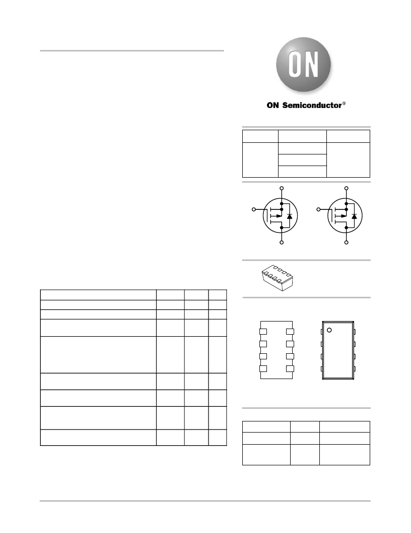
�G� 1�
�S� 1�
�G� 2�
�S� 2�
�Applications�
�?� Optimized� for� Battery� and� Load� Management� Applications� in�
�Portable� Equipment� such� as� MP3� Players,� Cell� Phones,� Digital�
�Cameras,� Personal� Digital� Assistant� and� other� Portable� Applications�
�?� Charge� Control� in� Battery� Chargers�
�?� Buck� and� Boost� Converters�
�MAXIMUM� RATINGS� (T� J� =� 25� °� C� unless� otherwise� noted)�
�D� 1�
�P?Channel� MOSFET�
�D� 2�
�P?Channel� MOSFET�
�ChipFET�
�CASE� 1206A�
�STYLE� 2�
�Rating�
�Symbol�
�Value�
�Unit�
�Drain?to?Source� Voltage�
�Gate?to?Source� Voltage� ?� Continuous�
�Drain� Current� ?� Continuous�
�V� DSS�
�V� GS�
�I� D�
�?8.0�
�"� 8.0�
�?3.4�
�V�
�V�
�A�
�PIN�
�CONNECTIONS�
�MARKING�
�DIAGRAM�
�?� 5� seconds�
�I� D�
�?4.6�
�D� 1� 8�
�1� S� 1�
�1�
�8�
�Total� Power� Dissipation�
�Continuous� @� T� A� =� 25� °� C�
�(5� sec)� @� T� A� =� 25� °� C�
�Continuous� @� 85� °� C�
�(5� sec)� @� 85� °� C�
�P� D�
�1.1�
�2.1�
�0.6�
�1.1�
�W�
�D� 1� 7�
�D� 2� 6�
�D� 2� 5�
�2� G� 1�
�3� S� 2�
�4� G� 2�
�2�
�3�
�4�
�7�
�6�
�5�
�Operating� Junction� and� Storage� Temperature�
�Range�
�T� J� ,� T� stg�
�?55� to�
�+150�
�°� C�
�D5� =� Specific� Device� Code�
�Continuous� Source� Current�
�(Diode� Conduction)�
�Thermal� Resistance� (Note� 1)�
�Junction?to?Ambient,� 5� sec�
�Junction?to?Ambient,� Continuous�
�Is�
�R� q� JA�
�R� q� JA�
�?1.1�
�60�
�113�
�A�
�°� C/W�
�M� =� Month� Code�
�G�
�=� Pb?Free� Package�
�ORDERING� INFORMATION�
�Device� Package� Shipping� ?�
�Maximum� Lead� Temperature� for� Soldering�
�Purposes,� 1/8� ″� from� case� for� 10� seconds�
�T� L�
�260�
�°� C�
�NTHD2102PT1�
�ChipFET�
�3000/Tape� &� Reel�
�Maximum� ratings� are� those� values� beyond� which� device� damage� can� occur.�
�Maximum� ratings� applied� to� the� device� are� individual� stress� limit� values� (not�
�normal� operating� conditions)� and� are� not� valid� simultaneously.� If� these� limits� are�
�NTHD2102PT1G�
�ChipFET�
�(Pb?Free)�
�3000/Tape� &� Reel�
�exceeded,� device� functional� operation� is� not� implied,� damage� may� occur� and�
�reliability� may� be� affected.�
�1.� Surface� Mounted� on� FR4� Board� using� 1� in� sq� pad� size� (Cu� area� =� 1.27� in� sq�
�[1� oz]� including� traces).�
�?For� information� on� tape� and� reel� specifications,�
�including� part� orientation� and� tape� sizes,� please�
�refer� to� our� Tape� and� Reel� Packaging� Specifications�
�Brochure,� BRD8011/D.�
�?� Semiconductor� Components� Industries,� LLC,� 2005�
�November,� 2005� ?� Rev.� 5�
�1�
�Publication� Order� Number:�
�NTHD2102P/D�
�发布紧急采购,3分钟左右您将得到回复。
相关PDF资料
NTHD2110TT1G
MOSFET P-CH 12V 4.5A CHIPFET
NTHD3100CT3G
MOSFET N/P-CH COMPL 20V CHIPFET
NTHD3101FT3G
MOSFET P-CH 20V 3.2A CHIPFET
NTHD3102CT1G
MOSFET N/P-CH COMPL 20V CHIPFET
NTHD3133PFT3G
MOSFET P-CH SGL 20V CHIPFET
NTHD4102PT3G
MOSFET P-CH DUAL 20V CHIPFET
NTHD4401PT3G
MOSFET 2P-CH 20V 2.1A CHIPFET
NTHD4502NT1
MOSFET N-CHAN DUAL 30V CHIPFET
相关代理商/技术参数
NTHD2110T
制造商:ONSEMI 制造商全称:ON Semiconductor 功能描述:Power MOSFET -12 V, -6.4 A, Single P-Channel +TVS, ChipFET? Package
NTHD2110TT1G
功能描述:MOSFET P-CH 12V 4.5A CHIPFET RoHS:是 类别:分离式半导体产品 >> FET - 单 系列:- 标准包装:1,000 系列:MESH OVERLAY™ FET 型:MOSFET N 通道,金属氧化物 FET 特点:逻辑电平门 漏极至源极电压(Vdss):200V 电流 - 连续漏极(Id) @ 25° C:18A 开态Rds(最大)@ Id, Vgs @ 25° C:180 毫欧 @ 9A,10V Id 时的 Vgs(th)(最大):4V @ 250µA 闸电荷(Qg) @ Vgs:72nC @ 10V 输入电容 (Ciss) @ Vds:1560pF @ 25V 功率 - 最大:40W 安装类型:通孔 封装/外壳:TO-220-3 整包 供应商设备封装:TO-220FP 包装:管件
NTHD3100C
制造商:ONSEMI 制造商全称:ON Semiconductor 功能描述:Power MOSFET 20 V, +3.9 A /−4.4 A, Complementary ChipFET
NTHD3100CT1
功能描述:MOSFET 20V +3.9A/-4.4A RoHS:否 制造商:STMicroelectronics 晶体管极性:N-Channel 汲极/源极击穿电压:650 V 闸/源击穿电压:25 V 漏极连续电流:130 A 电阻汲极/源极 RDS(导通):0.014 Ohms 配置:Single 最大工作温度: 安装风格:Through Hole 封装 / 箱体:Max247 封装:Tube
NTHD3100CT1G
功能描述:MOSFET 20V +3.9A/-4.4A Complementary RoHS:否 制造商:STMicroelectronics 晶体管极性:N-Channel 汲极/源极击穿电压:650 V 闸/源击穿电压:25 V 漏极连续电流:130 A 电阻汲极/源极 RDS(导通):0.014 Ohms 配置:Single 最大工作温度: 安装风格:Through Hole 封装 / 箱体:Max247 封装:Tube
NTHD3100CT3
功能描述:MOSFET 20V +3.9A/-4.4A RoHS:否 制造商:STMicroelectronics 晶体管极性:N-Channel 汲极/源极击穿电压:650 V 闸/源击穿电压:25 V 漏极连续电流:130 A 电阻汲极/源极 RDS(导通):0.014 Ohms 配置:Single 最大工作温度: 安装风格:Through Hole 封装 / 箱体:Max247 封装:Tube
NTHD3100CT3G
功能描述:MOSFET 20V +3.9A/-4.4A Complementary RoHS:否 制造商:STMicroelectronics 晶体管极性:N-Channel 汲极/源极击穿电压:650 V 闸/源击穿电压:25 V 漏极连续电流:130 A 电阻汲极/源极 RDS(导通):0.014 Ohms 配置:Single 最大工作温度: 安装风格:Through Hole 封装 / 箱体:Max247 封装:Tube
NTHD3100F
制造商:ONSEMI 制造商全称:ON Semiconductor 功能描述:Typical Uses for FETKY Devices